LTC4268-1
38
42681fc
Power MOSFET Selection
The power MOSFETs are selected primarily on the criteria of
on
resistance R
DS(ON)
, input capacitance, drain-to-source
breakdown voltage (BV
DSS
), maximum gate voltage (V
GS
)
and maximum drain current (ID
(MAX)
).
For the primary-side power MOSFET, the peak current is:
I
PK(PRI)
=
P
IN
V
IN(MIN)
DC
MAX
1+
X
MIN
2
?/DIV>
?/DIV>
?/DIV>
?/DIV>
?/DIV>
?/DIV>
where X
MIN
is peak-to-peak current ratio as defined
earlier. For each secondary-side power MOSFET, the peak
current is:
I
PK(SEC)
=
I
OUT
1DC
MAX
1+
X
MIN
2
?/DIV>
?/DIV>

?/DIV>
?/DIV>
?/DIV>
?/DIV>
Select a primary-side power MOSFET with a BV
DSS
greater
than:
BV
DSS
eI
PK
L
LKG
C
P
+ V
IN(MAX)
+
V
OUT(MAX)
N
SP
where N
SP
reflects the turns ratio of that secondary-to
primary winding. L
LKG
is the primary-side leakage induc-
tance and C
P
is the primary-side capacitance (mostly from
the drain capacitance (C
OSS
) of the primary-side power
MOSFET). A snubber may be added to reduce the leakage
inductance as discussed.
For each secondary-side power MOSFET, the BV
DSS
should
be greater than:
BV
DSS
e V
OUT
+ V
IN(MAX)
" N
SP
applicaTions inForMaTion
Choose the primary side MOSFET R
DS(ON)
at the nominal
gate drive voltage (7.5V). The secondary side MOSFET
gate drive voltage depends on the gate drive method.
Primary side power MOSFET RMS current is given by:
I
RMS(PRI)
=
P
IN
V
IN(MIN)
DC
MAX
For each secondary-side power MOSFET RMS current is
given by:
I
RMS(SEC)
=
I
OUT
1DC
MAX
Calculate MOSFET power dissipation next. Because the
primary-side power MOSFET operates at high V
DS
, a
transition power loss term is included for accuracy. C
MILLER
is the most critical parameter in determining the transition
loss, but is not directly specified on the data sheets.
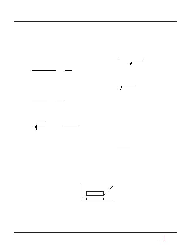
C
MILLER
is calculated from the gate charge curve included
on most MOSFET data sheets (Figure 17).
The flat portion of the curve is the result of the Miller
(gate-to-drain) capacitance as the drain voltage drops.
The Miller capacitance is computed as:
C
MILLER
=
Q
B
Q
A
V
DS
The curve is done for a given V
DS
. The Miller capacitance
for different V
DS
voltages are estimated by multiplying the
computed C
MILLER
by the ratio of the application V
DS
to
the curve specified V
DS
.
Q
A
V
GS
a
b
42681 F18
Q
B
MILLER EFFECT
GATE CHARGE (Q
G
)
Figure 18. Gate Charge Curve
发布紧急采购,3分钟左右您将得到回复。
相关PDF资料
LTC4274CUHF#PBF
IC CONTROLLER POE 38-QFN
LTC4280CUFD#PBF
IC CONTROLLER HOT SWAP QFN-24
LTC4300-1IMS8#TRPBF
IC HOTSWAP 2WIRE BUS BUFFR 8MSOP
LTC4300A-2IMS8#TRPBF
IC BUFFER BUS 2WR HOTSWAP 8-MSOP
LTC4301IDD
IC BUFFER BUS HOTSWAP 2WR 8DFN
LTC4301LIDD#TRPBF
IC BUFFER BUS HOTSWAP 2WR 8DFN
LTC4302IMS-1#TRPBF
IC BUFFER 2-WIRE BUS 10-MSOP
LTC4303CDD#TRPBF
IC BUS BUFFER I2C 8-DFN
相关代理商/技术参数
LTC4268IDKD-1#TRPBF
功能描述:IC PD HIGH POWER W/CNTRL 32-DFN RoHS:是 类别:集成电路 (IC) >> PMIC - 热交换 系列:- 产品培训模块:Obsolescence Mitigation Program 标准包装:100 系列:- 类型:热插拔开关 应用:通用 内部开关:是 电流限制:可调 电源电压:9 V ~ 13.2 V 工作温度:-40°C ~ 150°C 安装类型:表面贴装 封装/外壳:10-WFDFN 裸露焊盘 供应商设备封装:10-TDFN-EP(3x3) 包装:管件
LTC4268IDKD-1-PBF
制造商:LINER 制造商全称:Linear Technology 功能描述:High Power PD with Synchronous NoOpto Flyback Controller
LTC4268IDKD-1-TR
制造商:LINER 制造商全称:Linear Technology 功能描述:High Power PD with Synchronous NoOpto Flyback Controller
LTC4268IDKD-1-TRPBF
制造商:LINER 制造商全称:Linear Technology 功能描述:High Power PD with Synchronous NoOpto Flyback Controller
LTC4269-1
制造商:LINER 制造商全称:Linear Technology 功能描述:IEEE 802.3at PD with Synchronous No-Opto Flyback Controller
LTC4269-2
制造商:LINER 制造商全称:Linear Technology 功能描述:IEEE 802.3at High Power PD and Synchronous Forward Controller with AUX Support
LTC4269CDKD-1#PBF
功能描述:IC PD/OPTO FLYBACK CTRLR 32-DFN RoHS:是 类别:集成电路 (IC) >> PMIC - 热交换 系列:- 标准包装:50 系列:- 类型:热交换控制器 应用:-48V 远程电力系统,AdvancedTCA ? 系统,高可用性 内部开关:无 电流限制:可调 电源电压:11.5 V ~ 14.5 V 工作温度:-40°C ~ 85°C 安装类型:表面贴装 封装/外壳:10-TFSOP,10-MSOP(0.118",3.00mm 宽) 供应商设备封装:10-MSOP 包装:管件
LTC4269CDKD-1#TRPBF
功能描述:IC PD/OPTO FLYBACK CTRLR 32-DFN RoHS:是 类别:集成电路 (IC) >> PMIC - 热交换 系列:- 产品培训模块:Obsolescence Mitigation Program 标准包装:100 系列:- 类型:热插拔开关 应用:通用 内部开关:是 电流限制:可调 电源电压:9 V ~ 13.2 V 工作温度:-40°C ~ 150°C 安装类型:表面贴装 封装/外壳:10-WFDFN 裸露焊盘 供应商设备封装:10-TDFN-EP(3x3) 包装:管件
